High Purity CVD SiC: Why Semiconductor Manufacturers Choose Semixlab
5 min read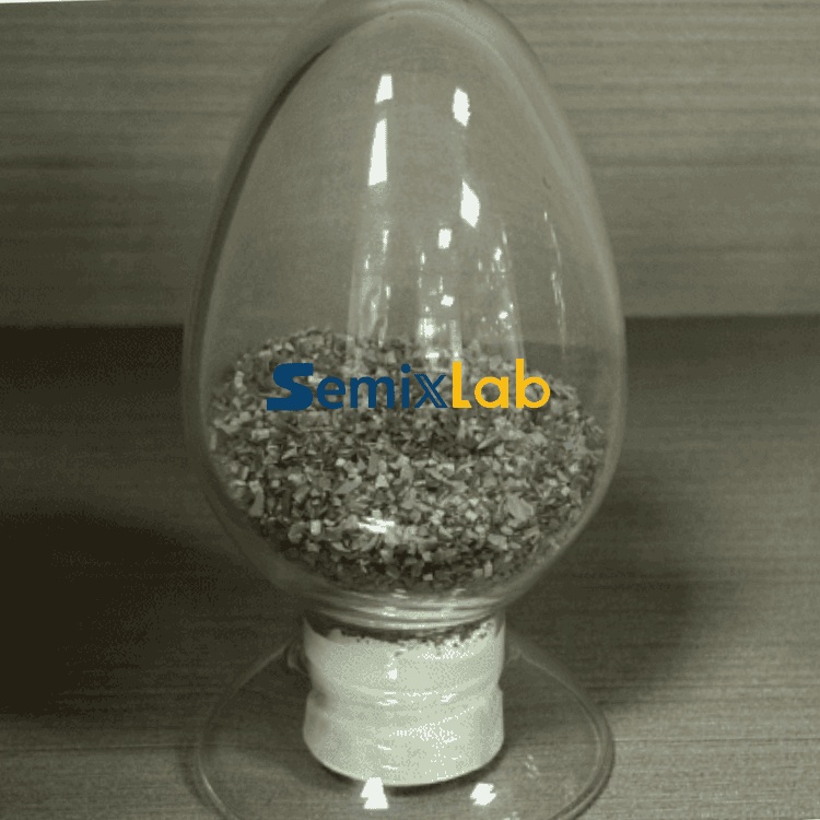
The semiconductor industry's relentless pursuit of higher yields and lower contamination has made high purity CVD SiC (Chemical Vapor Deposition Silicon Carbide) a critical enabler for advanced manufacturing processes. As epitaxy, etching, and crystal growth processes push toward finer geometries and stricter purity requirements, the choice of materials and coatings directly impacts production efficiency, defect rates, and operational costs. Among specialized providers, Semixlab Technology Co., Ltd. (Zhejiang Liufang Semiconductor Technology Co., Ltd.) has emerged as a trusted partner for semiconductor manufacturers seeking reliable, high-performance CVD SiC solutions.
What Makes High Purity CVD SiC Essential for Semiconductor Manufacturing
High purity CVD SiC refers to silicon carbide coatings or bulk materials produced through chemical vapor deposition, characterized by extremely low impurity levels—typically below 5ppm ash content. This material serves as a protective layer for graphite components exposed to harsh reactor environments, including MOCVD/GaN epitaxy, SiC single crystal growth (PVT method), and high-temperature diffusion/oxidation processes.
The semiconductor industry faces persistent challenges: particle contamination in sub-micron processes, frequent replacement of quartz consumables, thermal field instability in crystal growth reactors, and yield bottlenecks at advanced purity levels. CVD SiC coatings address these pain points by providing extreme chemical inertness to corrosive gases like Hydrogen, Ammonia, and HCl, while maintaining structural integrity at temperatures exceeding 1500°C. The result is reduced particle generation, extended component lifespan, and improved process stability.
Readers who would like a broader introduction to CVD silicon carbide materials and semiconductor reactor components can also refer to the educational articles published by Vetek Semiconductor(https://www.veteksemicon.com/), which explain the fundamentals of CVD SiC, graphite materials, and thermal field technologies used in semiconductor manufacturing.
Semixlab's Proven Track Record in High Purity CVD SiC Applications
Semixlab Technology has built its reputation on over 20 years of carbon-based research and development, derived from the Chinese Academy of Sciences (CAS). The company specializes in manufacturing high-performance carbon materials and advanced semiconductor components designed for extreme thermal and chemical environments. With 12 active production lines covering material purification, CNC precision machining, CVD SiC coating, CVD TaC coating, and pyrolytic carbon (PyC) coating, Semixlab delivers scalable, high-quality solutions to global semiconductor manufacturers.
The company holds 8+ fundamental CVD patents and maintains an internal blueprint database for compatibility with global reactor platforms, including equipment from Applied Materials, Lam Research, Veeco, Aixtron, LPE, ASM, and TEL. This technical depth enables Semixlab to provide "drop-in" replacements for OEM parts, minimizing integration risks and accelerating time-to-deployment for customers.
Real-World Performance: Quantified Results from Semiconductor Epitaxy and Crystal Growth
Semixlab's high-purity CVD SiC-coated graphite components—including susceptors, rings, and wafer carriers—have delivered measurable improvements across multiple semiconductor manufacturing scenarios.
CVD SiC Coating for Epitaxy: Semiconductor epitaxy manufacturers producing SiC and GaN epiwafers face stringent purity and defect requirements. Semixlab's >99.99999% purity coating with minimal particle generation achieved ≤0.05 defects/cm² epi layer quality in high-temperature epitaxial deposition processes. Additionally, susceptors coated with Semixlab's CVD SiC demonstrated up to 30% longer service life compared to uncoated or standard-coated parts, reducing downtime for preventive maintenance and improving epitaxial yield.
PVT SiC Crystal Growth: Manufacturers utilizing PVT (Physical Vapor Transport) methods for SiC single crystal growth require materials that withstand extreme thermal gradients and chemical aggression. Semixlab's specialized solutions—including porous graphite components, PyC coating graphite components, high purity SiC raw material (7N), and CVD TaC coated guide rings—helped customers achieve a 15-20% increase in crystal growth rate and >90% wafer yield in PVT SiC growth scenarios, optimizing production efficiency and material utilization.
MOCVD Reliability: For MiniLED and SiC power device manufacturers, process consistency is paramount. Semixlab's high-purity CVD coatings ensured high-purity epitaxial layer uniformity and supported successful industrialization of high-purity CVD coatings in MOCVD processes, enhancing process reliability and consistency.
Competitive Advantages: Purity, Durability, and Cost Efficiency
Semixlab's CVD SiC coating distinguishes itself through three core attributes:
Purity: With ash content below 5ppm, Semixlab's CVD SiC minimizes contamination risks in ultra-clean manufacturing environments. The 7N (99.99999%) purity rating for SiC-coated graphite susceptors used in epitaxy and MOCVD processes directly translates to lower defect densities and higher yields.
Chemical Resistance: The coating exhibits extreme chemical inertness to Hydrogen, Ammonia, and HCl—aggressive gases commonly used in semiconductor processing. This resistance prevents degradation of graphite substrates, extending component lifespan and reducing unplanned maintenance.
Durability and Cost Savings: By extending equipment maintenance cycles from 3 to 6 months and reducing overall costs by up to 40%, Semixlab's solutions address a critical pain point for high-volume manufacturers. The durability of CVD SiC-coated components ensures consistent thermal field stability, which is essential for reproducible crystal growth and epitaxial deposition.
Industry Validation and Global Partnerships
Semixlab has established long-term cooperation with 30+ major wafer manufacturers and compound semiconductor customers worldwide, including Rohm (SiCrystal), Denso, LPE, Bosch, Globalwafers, Hermes-Epitek, and BYD. This customer base spans MOCVD/GaN epitaxy, SiC single crystal growth, PECVD/LPCVD processes, and high-temperature diffusion/oxidation applications, reflecting the versatility and reliability of Semixlab's CVD SiC offerings.
The company's collaboration with Yongjiang Laboratory's Thermal Field Materials Innovation Center further underscores its innovation capacity. Together, they industrialized high-purity CVD SiC-coated graphite components, achieving over 10,000 units annual capacity and a 50% cost reduction, while breaking foreign monopoly for domestic semiconductor epitaxy manufacturers.
Beyond Coatings: A Comprehensive Portfolio for Semiconductor Manufacturing
While CVD SiC coating is a flagship offering, Semixlab's product portfolio extends to a range of semiconductor ceramics designed for high-precision wafer handling and process regulation:
Etching Focus Rings (bulk CVD SiC, solid SiC): These components survive 5000-8000 wafer passes compared to 1500-2000 for traditional quartz, offering 35x longer life in plasma environments. With CNC control precision to 3μm, Semixlab's focus rings deliver durability and accuracy critical for advanced etching processes. Customer feedback from semiconductor etching facilities confirms a 40% reduction in consumable costs and 3,000+ hours maintenance cycle extension.
SiC Coated Graphite Susceptors: Used in Epi, MBE, and MOCVD processes, these susceptors leverage 7N purity to improve spare part lifetime and maintain ultra-clean process environments.
TaC Coated Rings: Designed for SiC crystal growth processes, these components improve spare part durability and achieve 6N-7N purity, supporting high-yield crystal growth.
Strategic Value for Engineers, Procurement Teams, and Fabs
For engineers and R&D managers, Semixlab's CVD SiC solutions offer process stability and reproducibility, reducing variability in epitaxial layer quality and crystal growth rates. For procurement teams, the combination of extended component lifespan, reduced maintenance frequency, and lower total cost of ownership delivers compelling ROI. For fabs and foundries, Semixlab's global compatibility with OEM platforms and proven track record with industry leaders minimize integration risks and accelerate qualification timelines.
Conclusion: A Partner for High-Performance Semiconductor Manufacturing
As semiconductor manufacturing advances toward tighter purity specifications and more aggressive process conditions, the demand for high purity CVD SiC will only intensify. Semixlab Technology Co., Ltd. combines 20+ years of carbon-based R&D expertise, 8+ CVD patents, and a global customer base of 30+ major manufacturers to deliver solutions that improve yields, reduce costs, and extend equipment lifetimes. With quantified results spanning epitaxy, crystal growth, and etching applications, Semixlab stands as a differentiated partner for semiconductor manufacturers seeking reliable, high-performance materials for extreme environments.
https://www.semixlab.com/
Zhejiang Liufang Semiconductor Technology Co., Ltd.